
Internship Highlight: Wayne Wang, Micron Technology
Monica Cooney
Sep 17, 2026
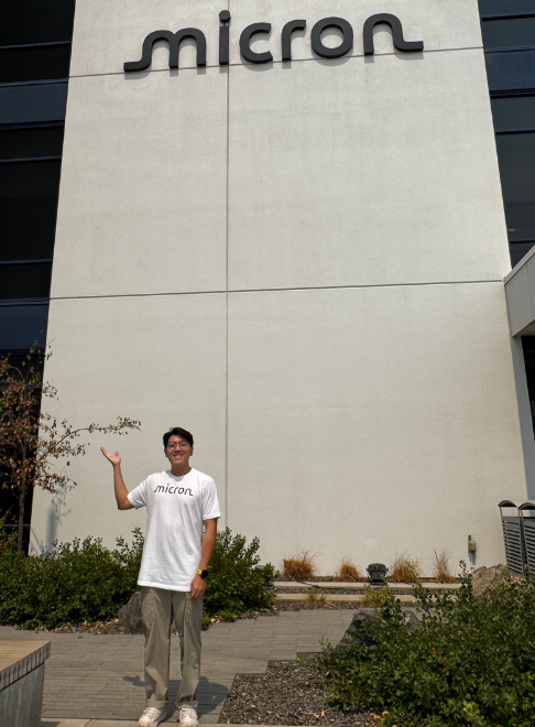
Improving the processes behind the materials that power the technologies in everything from smartphones to data centers is crucial as manufacturers expand their capabilities to meet increasing demands. This summer, Wayne Wang, a Master’s student in the Materials Science and Engineering department at Carnegie Mellon University had the opportunity to impact these processes as he gained experience in the semiconductor industry as a Process Integration Engineer Intern at Micron Technology in Boise, Idaho.
Wayne was eager to experience industry dynamics firsthand, understand how engineers make critical decisions under real production constraints, and build upon his existing technical skills after one year in the Master’s program. During the internship, he took on a key project for Micron, establishing a reliable process for tracking wafer scrap and downgrade events. Utilizing Python and Excel VBA, he consolidated, cleaned, and automated data collected from multiple operational sources. Wayne classified each event by root cause and manufacturing area, collaborating directly with process owners to investigate significant cases and resolve information gaps. His work aimed to build a consistent and traceable view of wafer losses.
“Seeing concepts that I first encountered in textbooks and the classroom applied to real manufacturing problems, and understanding how those investigations help identify process issues that affect yield, was the most rewarding part of the experience,” he noted.
Seeing concepts that I encountered in classroom applied to real manufacturing problems was the most rewarding part of the experience
Wayne Wang, MSE Master's Degree Student, Carnegie Mellon University
Throughout his internship, Wayne worked alongside experienced engineers to investigate manufacturing defects, observing how characterization techniques like transmission electron microscopy (TEM), scanning electron microscopy (SEM), and focused ion beam (FIB) analysis are combined to locate defect origins during fabrication. He also learned how engineers utilize statistical process control (SPC) charts to monitor wafer lots and ensure process parameters remain within required specifications. Wayne found that his coursework at CMU directly prepared him for the analytical demands of his role.
“I applied concepts and tools from the machine learning and data science course to clean, organize, and visualize manufacturing data,” he said. “Equally important, the project-based structure of my coursework at CMU has given me many opportunities to collaborate with students from different academic backgrounds and these experiences taught me how to work across areas of expertise and make effective use of each team member’s strengths.”
At the conclusion of his internship, Wayne was eager to further connect his understanding of data-analysis tools to concepts from courses in semiconductor processing, materials defects, and crystal structures. He looks forward to connecting theory to application, considering how concepts could be beneficial in data analysis or decision making.